

Glass created by humans dates back thousands of years. However, it is now on the verge of being utilized in the AI chips found in the newest and most extensive data centers globally. This year, a South Korean firm named Absolics plans to initiate the commercial manufacturing of unique glass panels aimed at enhancing the power and energy efficiency of next-generation computing hardware. Other corporations, such as Intel, are also advancing in this field. If everything proceeds smoothly, this glass technology could lessen the energy requirements of high-performance computing chips utilized within AI data centers—and it might eventually extend the same benefits to personal laptops and mobile devices, provided production costs decrease.
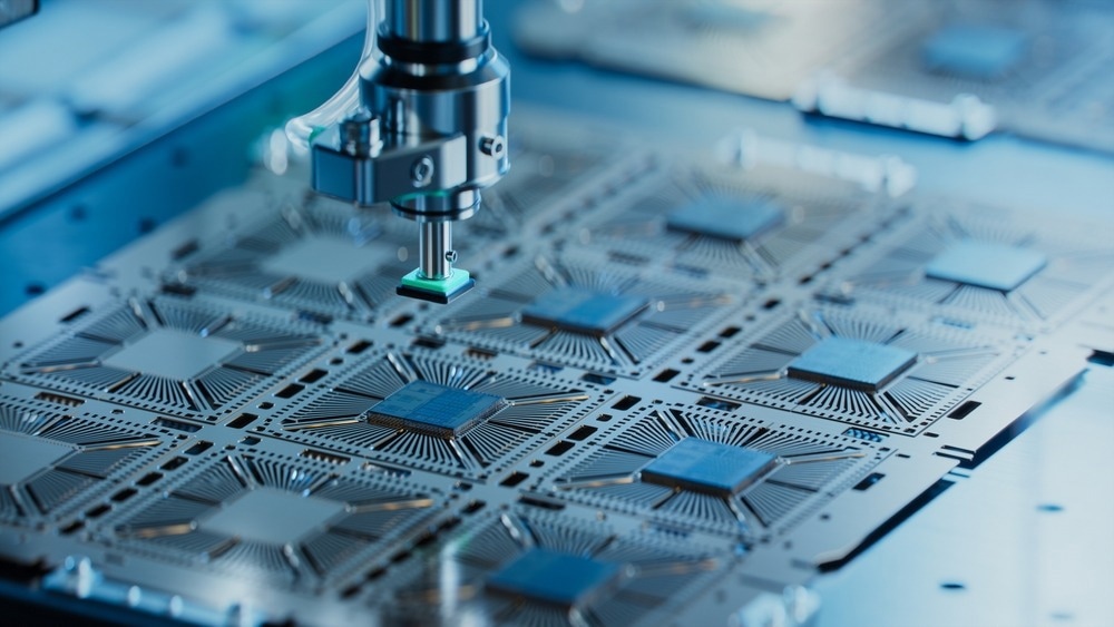
The concept is to utilize glass as the substrate, or layer, on which multiple silicon chips are interconnected. This method of “packaging” is increasingly favored for constructing computing hardware, as it allows engineers to integrate specialized chips crafted for particular functions into a unified system. Nevertheless, it poses challenges, such as the fact that high-performance chips can produce heat that warps the substrate they are built upon. This might result in misaligned components and could hinder the cooling efficiency of the chips, potentially leading to damage or early failure.
“With the rise in AI workloads and the expansion of package sizes, the industry faces very real mechanical limitations affecting the direction of high-performance computing,” states Deepak Kulkarni, a senior fellow at chip design company Advanced Micro Devices (AMD). “One of the most critical issues is warpage.”
This is where glass becomes crucial. It can better manage the extra heat than current substrates, enabling engineers to continually reduce the size of chip packages—which will enhance their speed and energy efficiency. It “opens up the possibility of scaling package footprints without encountering a mechanical barrier,” affirms Kulkarni.
Momentum is gathering for this transition. Absolics has completed a factory in the US dedicated to producing glass substrates for advanced chips and anticipates beginning commercial production this year. The US semiconductor manufacturer Intel is striving to integrate glass into its next-gen chip packages, and its research has prompted other companies within the chip packaging supply chain to invest in it as well. Early adopters include South Korean and Chinese firms. “Historically, this isn’t the first initiative to implement glass in semiconductor packaging,” remarks Bilal Hachemi, a senior tech and market analyst at market research firm Yole Group. “However, this time, the ecosystem is more robust and extensive; the demand for glass-based [technology] is more urgent.”
Brittle yet powerful
Since the 1990s, chip packaging has relied on organic substrates like fiberglass-reinforced epoxy, as noted by Rahul Manepalli, Intel’s vice president of advanced packaging. However, electrochemical issues restrict how closely designers can position drilled holes to form copper-coated signal and power connections linking the chips to the overall system. Chip designers must also consider the unpredictable shrinkage and warping organic substrates experience as chips heat up and cool down. “About a decade ago, we recognized that we would face limitations with organic substrates,” explains Manepalli.

Glass could potentially address many of these challenges. Its thermal stability might allow engineers to create connections ten times denser per millimeter than organic substrates, according to Manepalli. With these denser connections, Intel’s designers could fit 50% more silicon chips into the same package area, boosting computational ability. The denser connections also facilitate more efficient copper wire routing for power delivery to the chip. Additionally, because glass dissipates heat more effectively, this could enable chip designs that lower overall power consumption.
“The advantages of glass core substrates are irrefutable,” states Manepalli. “It’s evident that the merits will compel the industry to expedite this process, and we aspire to be among the first to implement it.”
However, working with glass introduces its own set of challenges. For instance, it is fragile. The glass substrates intended for data center chip packages consist of panels that are approximately 700 micrometers to 1.4 millimeters thick, making them vulnerable to cracks or shattering, according to Manepalli. Researchers at Intel and other institutions have dedicated years to discovering how to use alternative materials and specialized tools to safely integrate glass panels into semiconductor manufacturing processes.
Currently, Manepalli reports, Intel’s R&D teams are reliably producing glass panels and generating test chip packages that include glass—and in early 2025, they showcased that a functional device with a glass core substrate could boot the Windows operating system. This marks a notable enhancement from the early testing phases, when numerous glass panels would crack every few days, he adds.
Semiconductor manufacturers already employ glass for more limited applications, such as temporary support structures for silicon wafers. Nevertheless, the independent market research firm IDTechEx estimates that there exists a substantial market for glass substrates, one that could elevate the semiconductor market for glass from $1 billion in 2025 to as much as $4.4 billion by 2036.
If successful, this material may deliver added benefits. Glass can be manufactured to be remarkably smooth—up to 5,000 times smoother than organic substrates. This would eliminate defects that could emerge when layering metals onto semiconductors, according to Xiaoxi He, a research analyst at IDTechEx. Defects within these layers can degrade the performance of chips or even render them inoperable.
Glass could also facilitate faster data movement. Since the material can guide light, chip designers might utilize it to create high-speed signal pathways directly within the substrate. Glass “holds vast potential for the future of energy-efficient AI computing,” declares Kulkarni at AMD, as a light-based system could transmit signals using significantly less energy compared to the “power-hungry” copper pathways currently employed for signal transmission between chips in a package.
A panel pivot
Preliminary research concerning glass packaging commenced at the 3D Systems Packaging Research Center at the Georgia Institute of Technology in 2009. Ultimately, the university collaborated with Absolics, a branch of SKC, a South Korean firm that manufactures chemicals and advanced materials. In 2024, SKC established a semiconductor facility for glass substrate manufacturing in Covington, Georgia, and the partnership between Absolics and Georgia Tech was granted two awards in the same year, amounting to a total of $175 million—through the US government’s CHIPS for America initiative, created under President Joe Biden’s administration.

Absolics is now advancing towards commercialization; it aims to commence manufacturing limited quantities of glass substrates for clients this year. The company has spearheaded the way in commercializing glass substrates, claims Yongwon Lee, a research engineer at Georgia Tech not directly tied to the commercial alliance with Absolics.
Absolics states that its facility currently has the capability to produce a maximum of 12,000 square meters of glass panels annually. According to Lee’s estimates, this is sufficient to supply glass substrates for approximately 2 million to 3 million chip packages the size of Nvidia’s H100 GPU.
However, the company is not acting alone. Lee mentions that several major manufacturers, including Samsung Electronics, Samsung Electro-Mechanics, and LG Innotek, have “significantly accelerated” their research and pilot production initiatives in glass packaging over the last year. “This trend indicates that the glass substrate ecosystem is transforming from a solitary early mover into a more extensive industrial competition,” he remarks.
Other companies are adapting to take on more specialized roles within the glass substrate supply chain. In 2025, JNTC, a manufacturer of electrical connectors and tempered glass for electronics, established a facility in South Korea capable of producing 10,000 semi-finished glass panels monthly. These panels include drilled holes for vertical electrical connections, along with thin metal layers coated onto the glass, but they necessitate additional manufacturing steps before installation in chip packages.
Last year, the South Korean facility began accepting orders to supply semi-finished glass to specialized substrate companies as well as semiconductor manufacturers. The company plans to expand its production in 2026 and launch an additional manufacturing line in Vietnam in 2027. Such industry initiatives illustrate how rapidly glass substrate technology is transitioning from prototype stage to commercialization—and how numerous tech players are wagering that glass could serve as an unexpectedly robust foundation for the future of computing and AI.